Sputtering Targets Producers and Sputtering Targets Market Trend
The sputtering process is one of the main techniques for preparing electronic thin films. It uses ions generated by an ion source, which are accelerated and gathered in a high vacuum to form a high-speed ion beam stream that bombards the surface of a solid, where kinetic energy is exchanged between the ions and the atoms on the surface of the solid, causing the atoms on the surface of the solid to leave the solid and be deposited on the surface of the substrate. The bombarded solid is the raw material for depositing thin films by sputtering, called sputtering target.
The global sputtering targets market size was USD 13.6 billion in 2017, growing to USD 22.3 billion in 2022, with a CAGR of 10.4% from 2017 to 2022. The global sputtering targets market size is expected to grow to USD 35.5 billion in 2027, with a CAGR of 9.7% from 2022 to 2027.
Figure 2017-2027 Global Sputtering Targets Market Size (Billion USD) and CAGR

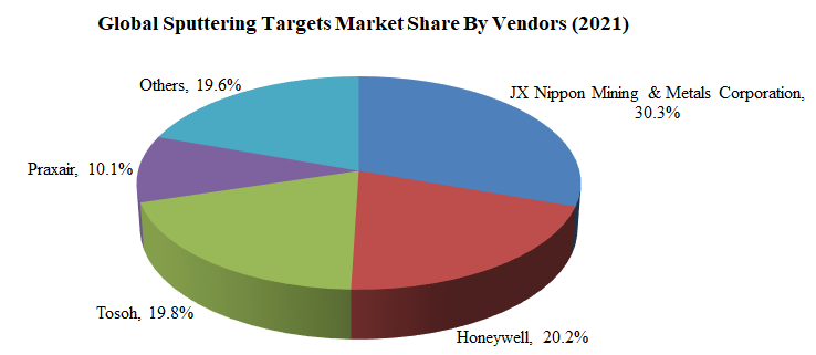
There are four major players in the global sputtering target market, namely JX Nippon Mining & Metals Corporation, Honeywell, Tosoh and Praxair, with market shares of 30.3%, 20.2%, 19.8% and 10.1% respectively, which together monopolize more than 80% of the global market share. There are also some smaller players include H.C. Starck, Heraeus, ULVAC, Plansee, Konfoong, GRIKIN, Fujian Acetron, Umicore and Longhua.
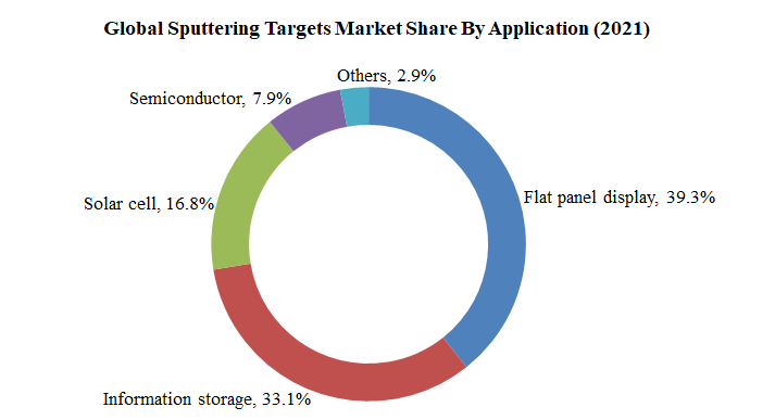
 The sputtering target can be used in semiconductor, flat panel display, solar cell and information storage. Flat panel display and information storage account for 39.3% and 33.1% respectively.